Samsung breaks ground on ₩6 trillion HBM packaging fab as Chungcheong investment rises to ₩144 trillion
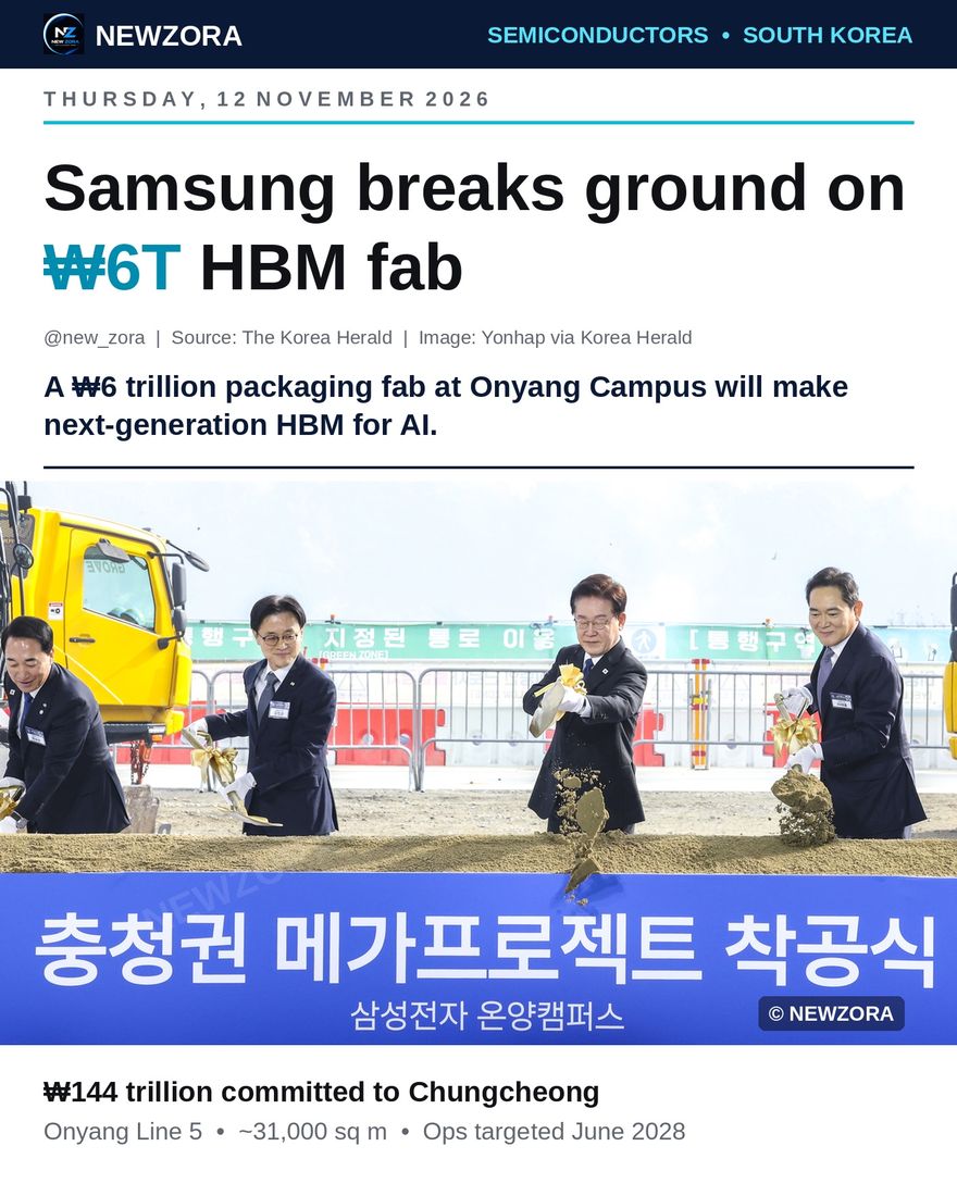
The ceremony also served as the occasion for Samsung to raise its total committed investment in the Chungcheong region to ₩144 trillion (approximately $108 billion), an increase of ₩4 trillion from the ₩140 trillion announced in July 2026. The commitment spans the group's principal affiliates and covers semiconductor packaging, displays, electronic components and batteries. A further ₩40 trillion in phased equipment investment is planned at the Onyang site, according to the reports of the ceremony.
The Onyang Line 5 facility
The new plant is a three-storey facility with a footprint of approximately 31,000 square metres. It will house advanced packaging lines for next-generation HBM, the stacked memory used alongside AI accelerators in data centres. Packaging, the process of assembling and interconnecting memory dies into finished modules, has become a central stage of the AI memory supply chain, because the performance of HBM depends as much on the density and quality of the interconnections as on the memory cells themselves.
The decision to move construction forward by approximately one year indicates the urgency with which Samsung is approaching the AI memory market. The company has not disclosed a specific production capacity or a customer list for the new line. Operations are targeted for June 2028, a date that should be read as a company target rather than a confirmed start of mass production, since the ramp of a packaging line depends on equipment installation, qualification and customer orders that have not been publicly specified.
A ₩144 trillion regional commitment
The raised regional commitment of ₩144 trillion is divided among four Samsung affiliates. Samsung Electronics accounts for ₩60 trillion, Samsung Display for ₩67 trillion, Samsung Electro-Mechanics for ₩8 trillion and Samsung SDI for ₩9 trillion. The figures are commitments announced by the group, not expenditure already incurred, and the reports do not give a single end date for the full programme.
The scale of the programme makes Chungcheong Province one of the largest single regional concentrations of Samsung investment. The additional ₩40 trillion in phased equipment investment at Onyang, announced alongside the groundbreaking, is separate from the ₩144 trillion total and will be spent over an unspecified period as the new packaging capacity is equipped.
Display investment in Asan
The largest single share of the commitment belongs to Samsung Display, whose ₩67 trillion includes the A7 OLED production line in Asan. Construction of that line began in October 2026, and mass production is targeted for the second half of 2029. The A7 line is intended to produce OLED panels for information technology products, extending the display affiliate's production base in the region alongside Samsung Electronics' semiconductor operations.
The grouping of semiconductor packaging and OLED display capacity in the same province reflects the geographic concentration of Samsung's manufacturing. Asan already hosts Samsung Display's principal OLED production, and the Onyang campus is the group's established site for semiconductor packaging and testing.
Attendance at the ceremony
President Lee Jae-myung attended the groundbreaking ceremony and spoke at the event, as did Samsung Electronics Chairman Lee Jae-yong. The presence of both the president and the group's chairman at a factory groundbreaking is a measure of the political and industrial weight attached to the investment, which the government has presented as part of South Korea's effort to hold its position in the global semiconductor supply chain.
Neither the government nor Samsung has disclosed further details of any public support attached to the project, and the reports of the ceremony do not specify whether the investment figures include government incentives.
Why it matters
High-bandwidth memory is one of the most supply-constrained components in the AI hardware market. Demand for AI accelerators has raised demand for HBM faster than producers have been able to add capacity, and packaging capacity, rather than wafer fabrication alone, has become a bottleneck. A dedicated packaging facility at Onyang addresses that bottleneck directly, and the accelerated construction schedule suggests Samsung expects demand to remain strong through the end of the decade.
The broader ₩144 trillion commitment also signals that Samsung intends to compete across the full stack of AI-era hardware: memory packaging at Samsung Electronics, displays at Samsung Display, substrates and components at Samsung Electro-Mechanics, and batteries at Samsung SDI. Whether the programme delivers its stated investment on schedule will depend on demand for AI hardware, the pace of construction and equipment installation, and the group's own capital allocation in the years ahead.
What is next
The immediate milestone is the construction of the three-storey plant at Onyang, with operations targeted for June 2028. The A7 OLED line in Asan is scheduled to reach mass production in the second half of 2029. The phased ₩40 trillion equipment investment at Onyang will follow as the packaging lines are fitted out. Further detail on capacity, customers and the timing of equipment spending has not been disclosed.